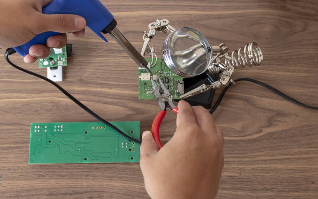
PCBs are one of the most common devices that you will see in the electronic world. These boards eliminate the various wires and breadboards and thus reduce your device’s size. In this article, we will learn how to make a circuit board for kids at home.
What is a circuit board?
A PCB or a printed circuit board provides mechanical support and connects the various electronic parts using pads, conductive tracks, and other such elements that are etched copper sheets and are laminated to form non-conductive substrates.
A PCB has a pre-designed copper track present on the conducting sheets. These tracks decrease the wirings needed and thus reduce the chances of faults occurring due to the presence of loose connections. Just place all the components of a PCB together and solder them.
How To Make A PCB At Home?
Preparing a PCB at home is quite easy. Follow the below-mentioned step to create one for yourself.
PCB Design:
To design a PCB you need to convert the circuit’s schematic diagram to a layout for a PCB. This is done using the software. There is numerous open-source software available in the market that helps in PCB Manufacturing design.
STEP 1: Take a printout of the circuit board layout
After preparing the PCB design, you need to take its print out using a laser printer on an A4 paper. Remember the following points:
- Take a mirror print out
- Select the print in black
- Make sure the printout comes out of the glossy end of the paper.
STEP 2: Cut a Copper board for the PCB
Now, cut a copper board as per the size of the PCB layout with the help of a cutter or a hacksaw. Then, rub the copper end of the PCB with the help of steel wool. It will help to remove the oxide layer of copper and also the photoresist layer.
STEP 3: Transfer the PCB Print onto the Copper Plate
Transfer the layout on a copper plate. Remember to flip the top layer horizontally. Now put the copper surface on the printed layout. Make sure the board is aligned along the layout’s borders and use tapes to keep the board in the correct position.
STEP 4: Move An Iron On The Paper To Transfer It To The PCB Plate
Now iron the copper side and then heat your electric iron. Put the arrangement on a wooden table and keep the photo paper on it. With the help of pliers, hold one end and keep it in the correct position. Now, put the hot iron on it for ten seconds. Move the iron a bit while applying a small pressure. The heat from the electric iron will transfer the ink from the paper onto the copper plate.
CAUTION: Make sure not to touch the hot surface of iron directly.
After ironing, keep the plate in lukewarm water for at least 10 minutes. Remove the dissolved paper gently.
Read More: PCB Design Tips Every Engineer and Hobbyist Should Know
STEP 5: Etching the Plate
You need to be careful while performing this step. Make sure you wear rubber gloves while doing this step. Place a newspaper on the bottom to make sure that the etching solution does not spill on your floor.
Fill up a plastic box with water. Put two to three teaspoons of ferric chloride solution in water and now put the PCB in this solution. This chemical will react with the copper and remove any dirt present on the PCBs surface.
STEP 6: Cleaning the plate, Disposal of the etching solution, and Giving Final Touches for the Circuit Board
Carefully dispose of the etching solution. It is toxic to numerous water organisms. Do not put it into the sink once you are done. Instead, dilute the solution and then dispose of it in a gutter nearby your home.
Now, with the help of a few drops of nail polish remover on a cotton ball, remove the ink present on the plate. This will expose the copper surface to you. Rinse the PCB carefully and then dry it with a soft cotton cloth. Trim the ends and then smoothen them with sandpaper. With this step done, you have your PCB ready to use.


