OLED (Organic Light Emitting Diode) – as the OLED definition we can accept that it’s a type of light emitting diode used as a superficial light source. Typically they are used for building flexible displays, TVs or other portable devices. OLEDs implemented into displays make them very thin due to the lack of need for their illumination because they generate light by itself. OLED symbol looks similar to the typical LED diode.
For the first time, the phenomenon of electroluminescence in organic materials was observed in 1950 by André Bernanose from France, who along with his colleagues from the University of Nancy noticed that after applying high alternating voltage to the the layer of organic material weak glow of light is emitted. Electroluminescence in polymer films was first discovered by Roger Partridge at the National Physical Laboratory in the United Kingdom. The first discoveries of electroluminescence in organic materials have taken place in 1960s and 1970s and they weren’t promising any more hope for their practical application in the future. This situation, however, changed in later years. One of the first organic compounds in which the phenomenon of light emission was discovered under the influence of the external electric field was polyphenylene vinylene. It turned out that this conductive polymer can emit green or yellow-green light under the influence of the applied voltage. The rapid development of OLED technology dates back to the year 2000. In October 2007, Sony has demonstrated the prototype TV made in OLED technology.
Organic word aforementioned in OLED definition stands for organic materials from which
several very thin layers of OLED structure are built. They are put on-top of each other.
These layers are called anode, cathode, conductive layer, emissive layer and base. It is possible to include a third organic layer for a more efficient transfering of electrons from the cathode to the emissive layer. A typical manufacturing process of OLED is done in the following order:
- The substrate is applied to the anode.
- The layer on the anode is specifically formed to be able to transfport holes.
- Application of the “n” -type conductive layer.
- “p” –type emissive layer is made through placing layer on-top of the conductive layer.
- Transport layer for electrons is applied.
- Cathode is placed on-top of previously made structure.
The thickness of the layers of the OLED technology does not exceed 500nm.
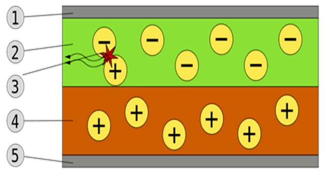
 Structure of OLED: 1. Cathode (-), 2. Emissive layer, 3. Emission of radiation, 4. Conductive layer, 5. Anode (source Wikipedia)
OLED operating principle is as follows: To start emitting light from OLED, it’s firstly needed to apply correct voltage to it’s structure. The electrons are then moving from cathode to anode – electrons from the cathode pass into the emissive layer and holes will pass from anode (anode will retrieve electrons from the conductive layer). Therefore junction will be forward-biased. While in forward-bias state, emissive layer will be charged negatively. Conductive layer is positively charged due to the presence of excess holes (positive charge-carriers). The mutual attraction of electrons and holes in the emissive layer arises due to the occurrence of electrostatic interaction phenomenon. After that the recombination phenomenon starts occuring – connection of a pair of particles with opposite electrical charges. Energy released during recombination causes the emission of light.
Again, according to OLED definition it can emit more or less light. This depends on the voltage that is applied to that diode. But we need to keep in mind that brighter light means greater power consumption. The color of this light depends on the type of the organic layer of material used in emissive layer in the diode. It will be lit only when junction is forward-biased (reverse-bias won’t work).
Advantages and disadvantages of using OLEDs – usage of OLED technology in the construction of any display has both advantages and disadvantages. As its advantages we can put:
- it is possible to produce flexible displays or sewn-screens e.g. in clothing due to the possibility of applying the organic material on a flexible substrate,
- low weight and display thickness,
- reduced manufacturing costs – lack of backlighting, non-complex construction and fewer layers of the display,
- greater brightness and color scale than in LCD technology that is caused by spontaneous, unfiltered light emission of OLEDs,
- backlight is not required what leads to lower OLED power consumption – black colour is perfectly black,
- view angle is almost unlimited,
- faster response time (~ 0,01ms) compared to LCD technology (2-12ms).
Among OLED Disadvantages one can find:
- short lifespan of organic materials – blue OLED has the shortest lifetime among the three RGB colors (Red, Green, Blue): about 5000-14000h. Red and green OLEDs could work between 46,000-230,000h, so blue OLED can be seen as a problem that will still need a better solution,
- current consumption – scientists have observed greater power consumption while displaying white and bright elements e.g. while browsing Web, therefore it may be uneconomical for some applications,
- susceptibility to environmental factors – organic materials that are used in OLED structure are particularly sensitive to environmental factors. In case of mechanical damage to the matrix display, water or humidity can easily destroy it. Using an additional protection would be a great idea,
- limited patents – the development of OLED technology is dependent on companies that have ownership of patents (e.g. Eastman Kodak Company), which require the payment of license-fees to allow taking any „further steps” in this area.


